![]()
Photoresist Market Size, Share and Research Report By Application (Semiconductor & IC, and LCD), By Ancillary Type (Anti-reflective Coating, Remover, Developer)
NEW YORK,, NY, UNITED STATES, July 3, 2026 /EINPresswire.com/ — The global Photoresist Market is entering a decade of structurally accelerated growth, propelled by the semiconductor industry’s relentless migration toward extreme ultraviolet lithography, the proliferation of AI and high-performance computing chip programs demanding sub-3 nm process nodes, and a global wave of government-backed fab construction programs that are reshaping resist supply chains across North America, Europe, and Asia-Pacific.
Photoresist chemistries spanning ArF immersion formulations, EUV metal-oxide dry resists, KrF platforms, and specialty thick-film packaging resists have become the critical consumable frontier where semiconductor node advancement is won or lost, making this one of the most technically demanding and high-value materials segments in the global semiconductor supply chain.
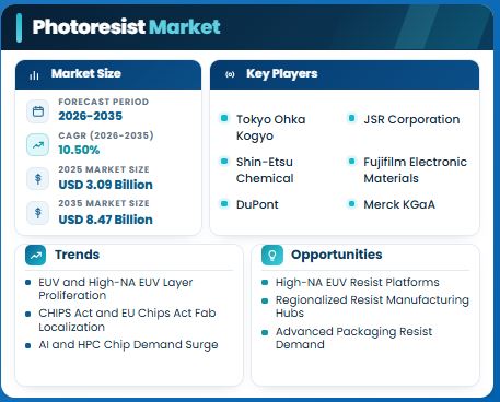
The global Photoresist Market reached an estimated USD 3.09 billion in 2025 and is projected to grow from USD 3.45 billion in 2026 to USD 8.47 billion by 2035, registering a CAGR of 10.50% across the 2026–2035 forecast period.
Get Full PDF Sample Copy of Report: (Including Full TOC, List of Tables & Figures, Chart) @
https://www.marketresearchfuture.com/sample_request/17758
Key Drivers Fueling Market Growth:
The convergence of three distinct technological and policy-driven pillars is accelerating the expansion of the Photoresist Market:
➤ EUV and High-NA EUV Layer Proliferation:
The most powerful structural driver in the Photoresist Market is the exponential growth in EUV lithography layer counts as foundries advance to smaller process nodes. At the 7 nm node, leading foundries exposed approximately five EUV layers per wafer; at the 3 nm node this has risen to 15–20 layers per wafer, and sub-2 nm architectures will require 25 or more EUV exposures per device. ASML’s 0.55-NA high-NA EUV scanner entered pilot production at two leading-edge foundries in 2025, with over 20 tools projected to be installed across global leading-edge fabs by 2028.
Each high-NA tool demands metal-oxide resist platforms with advanced resolution capability and defectivity standards that chemically amplified predecessors cannot meet and EUV resists are priced three to five times higher per liter than ArF immersion formulations, making layer proliferation a compounding revenue driver that simultaneously expands consumption volume and premium price mix across the Photoresist Market.
➤ CHIPS Act and EU Chips Act Fab Localization:
Government-backed semiconductor localization programs are reshaping photoresist supply chains at a structural level. Preliminary CHIPS Act grants totaling over USD 36 billion have been awarded across 16 fab projects as of early 2025, encompassing TSMC’s Arizona campus, Samsung’s Taylor fab, Intel’s Ohio mega-site, and Micron’s New York and Idaho expansion facilities. Every new fab requires a localized resist supply ecosystem including blending, filtering, and analytical quality-control facilities within a 48-hour logistics radius compelling major resist suppliers including Tokyo Ohka Kogyo, Shin-Etsu Chemical, and JSR to announce or accelerate North American facility investments.
Europe’s EUR 43 billion EU Chips Act is driving a parallel localization wave, with Merck KGaA and JSR expanding European blending centers to serve TSMC Dresden, Intel Magdeburg, and STMicroelectronics-Global Foundries Crolles capacity additions. This structural reshoring of resist manufacturing infrastructure creates durable demand floors that extend well beyond individual fab ramp cycles.
➤ AI and HPC Chip Demand Surge Driving Advanced-Node Volume:
Global spending on AI-optimized semiconductors surpassed USD 70 billion in 2024, with hyperscale training-cluster roadmaps now specifying 2 nm and 1.4 nm process nodes for 2027–2029 tape-outs. AI accelerators and high-bandwidth memory chips produced at leading-edge nodes consume photoresist at disproportionately elevated rates due to larger die sizes, higher EUV layer counts, and stringent defectivity tolerances compared to mainstream node production.
This AI-driven advanced-node demand creates a sustained pull on the highest-value resist chemistry platforms in the Photoresist Market simultaneously inflating per-wafer resist consumption and shifting product mix toward premium EUV and high-NA metal-oxide formulations that command the industry’s highest gross margins.
Market Segmentation Analysis
To provide a granular understanding of the landscape, global market research highlights a comprehensive segmentation across several key domains:
By Photoresist Type
ArF Immersion: The largest resist type at 34.1% Photoresist Market share in 2025, serving the 7 nm through 28 nm process window that encompasses the majority of global wafer starts. These chemically amplified formulations benefit from decades of foundry optimization, delivering predictable process latitude, low defectivity, and broad multi-vendor qualification across leading foundries and IDMs worldwide.
EUV Metal-Oxide: The fastest-growing resist type at an 11.90% CAGR through 2035, driven by sub-5 nm logic and HBM memory node ramps. Metal-oxide platforms use inorganic tin-oxygen clusters that deliver higher EUV photon absorption and reduced shot-noise sensitivity compared to chemically amplified predecessors a chemistry architecture that becomes indispensable as leading foundries push past 3 nm into 2 nm and angstrom-class production nodes.
KrF: Expanding at an 8.9% CAGR through 2035, sustained by automotive-grade 28–65 nm semiconductor manufacturing and mature IoT node volume growth. The rise in average silicon content per vehicle from USD 600 in 2021 to over USD 1,000 in 2025 provides a reliable revenue floor for KrF resist consumption across automotive-focused foundry and IDM operations.
I-Line: Holding 15.8% of Photoresist Market revenue in 2025, serving power semiconductor, MEMS, and display driver IC manufacturing at mature nodes where process maturity and low cost-per-exposure outweigh resolution capability as primary selection criteria.
ArF Dry Film: Valued at USD 0.31 billion in 2025, serving legacy 45–65 nm production runs at cost-optimized mature foundries and IDM facilities where single-patterning ArF dry exposure remains the most economically efficient lithography approach.
G-Line: Valued at USD 0.14 billion in 2025, maintaining a niche Photoresist Market position in display panel patterning and thick-film applications requiring relatively coarse resolution at large substrate formats.
By Tone
Positive-Tone: The dominant segment at 76.3% of Photoresist Market revenue in 2025, reflecting the semiconductor industry’s standard development process architecture where exposed regions dissolve, making positive tone the default chemistry for most front-end lithography patterning sequences across logic, memory, and analog device manufacturing.
Negative-Tone: The fastest-growing tone segment at a 10.40% CAGR through 2035, propelled by advanced packaging redistribution layer patterning, 3D-NAND multi-patterning sequences, and EUV negative-tone development processes where cross-linking chemistry delivers superior pattern transfer fidelity and resist adhesion for high-aspect-ratio structure formation.
By Application
Semiconductors & ICs: The dominant application at 58.5% of Photoresist Market demand in 2025, driven by leading-edge logic, DRAM, 3D-NAND flash, and analog semiconductor manufacturing across global foundry and IDM fabrication facilities.
Advanced Packaging: The fastest-growing application at an 11.00% CAGR through 2035, driven by chiplet-based heterogeneous integration architectures requiring 3–5 additional lithography layers per device for redistribution, fan-out, and hybrid bonding processes each consuming thick-film and dry-film photoresists distinct from front-end chemistries.
Displays: Valued at USD 0.28 billion in 2025, serving OLED, micro-LED, and LCD panel patterning applications at Asia-Pacific display fab clusters, with demand growth tied to global display technology migration from LCD to OLED and emerging micro-LED architectures.
PCBs: Representing 7.2% of Photoresist Market share in 2025, sustained by 5G telecom infrastructure buildout, high-density interconnect PCB manufacturing, and automotive electronics board fabrication demanding fine-line photoimageable solder mask and etch-resist chemistries.
MEMS: Expanding at a 6.8% CAGR through 2035, driven by automotive inertial sensor, environmental sensor, and IoT microphone manufacturing programs requiring specialty thick-film resist platforms compatible with deep silicon etch and anodic bonding processes.
By Ancillary Type
Anti-Reflective Coatings (ARC): Critical underlayer chemistries that suppress reflected standing waves during EUV and ArF immersion exposure, enabling tighter critical dimension control and reduced pattern roughness a segment expanding in direct proportion to advanced-node EUV layer proliferation across leading foundries.
Developer: Specialty aqueous alkaline and organic solvent developer formulations that dissolve exposed or unexposed resist regions with high selectivity, precision, and uniformity with negative-tone development chemistries gaining share at EUV nodes as alternatives to standard TMAH-based positive developers.
Remover: Post-lithography strip chemistries for photoresist removal after etch or ion implantation, including dry plasma ash processes and specialty wet strip formulations for temperature-sensitive advanced-node device structures.
By End-User Industry
Electronics & Electricals: The dominant end-user category at 65.4% of Photoresist Market revenue in 2025, encompassing consumer electronics, computing platforms, data-center semiconductors, and telecommunications infrastructure IC manufacturing.
Automotive & Mobility: The fastest-growing end-user vertical at a 10.90% CAGR through 2035, driven by the rising average semiconductor content per vehicle exceeding USD 1,000 in 2025 and the global electric vehicle transition demanding power semiconductor, ADAS processor, and connectivity chip volume expansion at KrF and mature ArF nodes.
Aerospace & Defense: Valued at USD 0.11 billion in 2025, serving radiation-hardened IC and specialty compound semiconductor manufacturing for defense electronics and space applications with stringent process qualification and long-term supply continuity requirements.
Consumer Packaged Goods: Representing 5.1% of Photoresist Market share, driven by RFID tag manufacturing, smart packaging sensor integration, and barcode reader IC production at cost-optimized mature photoresist nodes.
Get access to the full description of the report @
https://www.marketresearchfuture.com/reports/photoresist-market-17758
➤ Regional Insights
Asia-Pacific: Commands 67.2% of Photoresist Market revenue in 2025, reflecting the region’s unmatched concentration of leading-edge and mature-node semiconductor fabrication capacity. Taiwan’s TSMC foundry cluster alone accounts for approximately 60% of global foundry revenue, generating the world’s largest single-concentration demand pool for advanced resist chemistries. South Korea’s Samsung and SK Hynix memory fabrication complexes drive substantial ArF immersion and EUV resist procurement for DRAM and 3D-NAND production.
North America: The fastest-growing Photoresist Market region at a 10.50% CAGR through 2035, anchored by the United States’ CHIPS Act-funded greenfield fab wave. TSMC’s Arizona campus, Samsung’s Taylor Texas facility, Intel’s Ohio and Arizona expansion programs, and Micron’s New York and Idaho DRAM fabs collectively represent more than 500,000 wafer-starts-per-month of incremental capacity entering production between 2025 and 2029 each requiring localized resist supply within a tight logistics window.
Europe: Valued at USD 0.38 billion in Photoresist Market revenue in 2025 and accelerating under the EUR 43 billion EU Chips Act. Germany leads European demand at 31.5% of regional share, anchored by Infineon’s Dresden 300 mm mega-fab and Bosch’s Reutlingen facility targeting automotive-grade 28–65 nm KrF and i-line resist consumption.
South America and Middle East & Africa: Represent nascent but strategically watched frontier Photoresist Market regions. South America generated 2.1% of global Photoresist Market revenue in 2025, led by Brazil’s consumer electronics PCB assembly corridor in Manaus. The Middle East & Africa contributed USD 0.08 billion in 2025, with Saudi Arabia’s Vision 2030 allocating investments toward domestic technology manufacturing feasibility studies and the UAE’s smart-city infrastructure generating niche demand for MEMS sensor resist products.
➤ Top Key Companies
The global Photoresist Market exhibits high concentration, with the top five suppliers Tokyo Ohka Kogyo, JSR Corporation, Shin-Etsu Chemical, Fujifilm Electronic Materials, and DuPont collectively holding an estimated 70–78% of global revenue.
✿Tokyo Ohka Kogyo (TOK, Japan): The global market share leader in photoresist at an estimated 18–22% revenue share, delivering a full-spectrum portfolio spanning ArF immersion, KrF, EUV metal-oxide resists, and ancillary materials with deep process-of-record qualifications across every major foundry and IDM globally.
✿JSR Corporation (Japan): A strategic EUV-first innovator holding 14–18% Photoresist Market revenue share, whose USD 6.2 billion take-private by the Japan Investment Corporation in March 2025 positions JSR’s Inpria metal-oxide EUV resist platform under government-aligned strategic ownership accelerating commercialization of the industry’s most advanced sub-3 nm resist chemistry.
✿Shin-Etsu Chemical (Japan): A vertically integrated global leader at 12–16% revenue share, combining proprietary resin synthesis capabilities with ArF immersion and KrF resist manufacturing including a 25% capacity expansion at its Naoetsu production plant in April 2024 to meet accelerating foundry demand.
✿Fujifilm Electronic Materials (Japan): A diversified Photoresist Market specialist at 8–12% revenue share, offering ArF immersion, i-line, and advanced packaging resist platforms across leading foundry, memory, and display panel manufacturing customers with a broad multi-application materials portfolio.
✿DuPont (US): A global electronic materials platform provider at 7–10% Photoresist Market revenue share, integrating ArF resist formulations with anti-reflective coatings and CMP slurries to deliver end-to-end lithography consumable ecosystem solutions for advanced logic and memory manufacturers.
✿Merck KGaA (Germany): A European anchor in the Photoresist Market at 5–8% revenue share through its AZ Electronic Materials brand, holding strong automotive-grade semiconductor node presence and expanding European blending center infrastructure to serve EU Chips Act-funded fab programs in Germany, France, and the Netherlands.
✿Dongjin Semichem (South Korea): A cost-competitive Korean photoresist specialist at 4–6% revenue share, serving Samsung and SK Hynix memory fabrication programs with KrF and i-line resist formulations qualifying as secondary-source alternatives across mature-node production layers.
✿Sumitomo Chemical (Japan): A chemical conglomerate with a 3–5% Photoresist Market revenue share through its electronic materials division, offering ArF immersion, i-line, and specialty resist platforms with the procurement reliability and supply continuity that long-qualification-cycle memory and automotive customers require.
✿Kempur Microelectronics (China): A scaling domestic Chinese photoresist supplier at 1–3% revenue share, serving China’s mature KrF and i-line node demand as the primary beneficiary of Beijing’s semiconductor self-sufficiency investment programs and the structural import substitution imperative created by Western export control regimes.
➤ Emerging Trends and Future Outlook:
The future of the Photoresist Market will be defined by three converging transformation vectors: AI-driven semiconductor demand sustaining an advanced-node supercycle, resist chemistry co-evolution tracking alongside gate-all-around and complementary FET transistor architectures, and sustainability mandates restructuring formulation strategies across the global supply base. Industry leaders are building resist development ecosystems where a foundry doesn’t simply procure a resist product, but co-develops application-specific formulation optimizations through long-cycle joint engineering programs with resist suppliers generating proprietary process-of-record chemistry platforms that create multi-year supplier lock-in and insulate leading resist manufacturers from commodity pricing pressure.
➤ FAQs
Q – How does the transition to high-NA EUV lithography structurally differentiate photoresist performance requirements from standard EUV processes, and what does this mean for supplier qualification dynamics?
Ans – High-NA EUV systems operating at 0.55 numerical aperture deliver a significantly smaller aerial image compared to standard 0.33-NA EUV scanners, requiring resists with lower activation energy thresholds, tighter defectivity tolerances at sub-20 nm critical dimensions, and resist film thicknesses typically reduced to approximately 20 nm approximately half the thickness of standard EUV resist coatings.
This thinning requirement demands entirely new underlayer and etch-transfer integration architectures, as resist etch selectivity at 20 nm thickness cannot match the pattern-transfer robustness of thicker standard EUV films
Q – What strategic criteria should photoresist suppliers prioritize when planning capacity and supply chain localization investments in response to the CHIPS Act and EU Chips Act fab construction wave?
Ans – Photoresist suppliers evaluating CHIPS Act and EU Chips Act localization investments must prioritize a 48-hour logistics radius from each anchor fab cluster as the primary site selection constraint leading foundries require on-hand resist inventory windows that cannot accommodate trans-Pacific or trans-Atlantic shipping lead times for critical production materials. Beyond logistics proximity, suppliers must assess the resist chemistry mix demanded by each fab’s target node and application portfolio an Arizona logic fab targeting sub-3 nm production demands EUV metal-oxide resist blending and quality-assurance capability, while a Texas memory facility requires ArF immersion and KrF capacity
➤➤➤ Discover More Insights with Market Research Future:
Robotic Window Cleaners Market-
https://www.marketresearchfuture.com/reports/robotic-window-cleaners-market-24361
Indian Mobile Components Manufacturing Assembly Market-
https://www.marketresearchfuture.com/reports/indian-mobile-components-manufacturing-assembly-market-24663
Unsecured Business Loans Market-
https://www.marketresearchfuture.com/reports/unsecured-business-loans-market-24673
Marine Cargo Insurance Market-
https://www.marketresearchfuture.com/reports/marine-cargo-insurance-market-24797
Forex Prepaid Card Market
https://www.marketresearchfuture.com/reports/forex-prepaid-card-market-24849
Television Tv Mount Market-
https://www.marketresearchfuture.com/reports/television-tv-mount-market-26465
Factoring Market-
https://www.marketresearchfuture.com/reports/factoring-market-29977
Dedicated Outdoor Air System Market-
https://www.marketresearchfuture.com/reports/dedicated-outdoor-air-system-market-30005
Data Center Generator Market-
https://www.marketresearchfuture.com/reports/data-center-generator-market-30113
Alternative Legal Service Providers Market-
https://www.marketresearchfuture.com/reports/alternative-legal-service-providers-market-31274
Sagar Kadam
Market Research Future
+1 628-258-0071
email us here
Legal Disclaimer:
EIN Presswire provides this news content “as is” without warranty of any kind. We do not accept any responsibility or liability
for the accuracy, content, images, videos, licenses, completeness, legality, or reliability of the information contained in this
article. If you have any complaints or copyright issues related to this article, kindly contact the author above.
![]()
Media gallery